- 您现在的位置:买卖IC网 > Sheet目录341 > MAX5092EVKIT+ (Maxim Integrated Products)KIT EVALUATION FOR MAX5092
�� �
�
�4V� to� 72V� Input� LDOs� with� Boost� Preregulator�
�P� DISS� includes� the� losses� in� the� boost� converter� opera-�
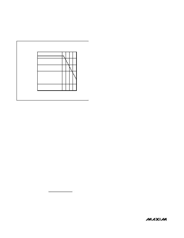
�MAXIMUM� POWER� DISSIPATION�
�vs.� AMBIENT� TEMPERATURE�
�3.0�
�2.5�
�2.0�
�1.5�
�1.0�
�0.5�
�0�
�-40� -25� -10� 5� 20� 35� 50� 65� 80� 95� 110� 125�
�AMBIENT� TEMPERATURE� (� °� C)�
�Figure� 8.� MAX5092/MAX5093� Package� Power� Dissipation�
�Maximum� Output� Current� (I� OUT_MAX� )�
�The� MAX5092_/MAX5093_� high� input� voltage� (+72V�
�max)� provides� up� to� 250mA� of� current� from� OUT.�
�Package� power-dissipation� limits� the� amount� of� output�
�current� available� for� a� given� input/output� voltage� and�
�ambient� temperature.� Figure� 8� depicts� the� maximum�
�power-dissipation� curve� for� the� devices.� The� graph�
�assumes� that� the� exposed� metal� pad� of� the� IC� package�
�is� soldered� to� the� PCB� copper� according� to� the� JEDEC�
�51� standard� (multilayer� board).� Use� Figure� 8� to� deter-�
�mine� the� allowable� package� dissipation� for� a� given�
�ambient� temperature.� Alternately,� use� the� following� for-�
�mula� to� calculate� the� allowable� package� dissipation�
�(P� DISS� )� in� watts:�
�tion� and� the� LDO� itself.� The� boost� converter� loss�
�P� LOSS(BST)� ,� depends� on� V� IN� ,� V� BSOUT� ,� and� I� OUT� .� See�
�the� Boost� Converter� Power� Loss� graphs� in� the� Typical�
�Operating� Characteristics� to� estimate� the� losses� at� a�
�given� V� IN� and� V� BSOUT� at� room� temperature.� At� a� higher�
�ambient� temperature� of� +105°C,� P� LOSS(BST)� increases�
�by� up� to� 20%� due� to� higher� R� DS-ON� and� switching� loss-�
�es� of� the� internal� boost� converter� MOSFET.� (Note:�
�I� OUT_MAX� must� be� less� than� 250mA).�
�PCB� Layout� Guidelines�
�Good� PCB� layout� and� routing� are� required� in� high-fre-�
�quency� switching� power� supplies� to� achieve� proper�
�regulation� and� stability.� It� is� strongly� recommended� that�
�the� evaluation� kit� PCB� layouts� be� followed� as� closely� as�
�possible.� Refer� to� the� MAX5092� EV� kit� for� an� example�
�layout.� Follow� these� guidelines� for� good� PCB� layout:�
�1)� For� SGND,� use� a� large� copper� plane� under� the� IC�
�and� solder� it� to� the� exposed� paddle.� To� effectively�
�use� this� copper� area� as� a� heat� exchanger� between�
�the� PCB� and� ambient,� expose� this� copper� area� on�
�the� top� and� bottom� side� of� the� PCB.� Do� not� make� a�
�direct� connection� from� the� EP� copper� plane� to� pin� 3�
�(SGND)� underneath� the� IC� so� as� to� minimize�
�ground� bounce.�
�2)� Isolate� the� power� components� and� high-current�
�path� from� the� sensitive� analog� circuit.�
�3)� Keep� the� high-current� paths� short,� especially� at� the�
�ground� terminals.� This� practice� is� essential� for� sta-�
�ble,� jitter-free� operation.�
�4)� Connect� the� return� terminals� of� input� capacitors�
�and� boost� output� capacitors� to� the� PGND_BST�
�power� ground� plane.� Connect� the� power� ground�
�For� T� A� ≤� +70°C:�
�P� DISS� =� 2.67�
�(PGND_BST)� and� signal� ground� (SGND)� planes�
�together� at� the� negative� terminal� of� the� input� capac-�
�itors.� Do� not� connect� them� anywhere� else.� Connect�
�For� +70°C� <� T� A� ≤� +125°C:�
�P� DISS� =� 2.67� -� (0.0333� x� (T� A� -� 70))�
�where� +70°C� <� T� A� ≤� +125°C� and� 0.0333W/°C� is� the�
�package� thermal� derating.� After� determining� the� allow-�
�able� package� dissipation,� calculate� the� maximum� out-�
�put� current� (I� OUT_MAX� )� using� the� following� formula:�
�PGND_LDO� ground� plane� to� SGND� ground� plane�
�at� a� single� point.�
�5)� Ensure� that� the� feedback� connections� are� short� and�
�direct.� Ensure� a� low-impedance� path� between�
�BSFB� and� SGND� to� limit� the� transient� at� BSFB� to�
�100mV.�
�I� OUT� _� MAX� =�
�P� DISS� ?� P� LOSS(BST)�
�V� IN� ?� V� OUT�
�6)� Route� high-speed� switching� nodes� away� from� the�
�sensitive� analog� areas.� Use� the� internal� PCB� layer�
�for� SGND� as� an� EMI� shield� to� keep� radiated� noise�
�away� from� the� IC,� feedback� dividers,� and� bypass�
�where� P� DISS� is� the� allowable� package� power� dissipa-�
�tion� and� P� LOSS(BST)� is� the� boost� converter� power� loss.�
�capacitors.�
�20�
�______________________________________________________________________________________�
�发布紧急采购,3分钟左右您将得到回复。
相关PDF资料
MAX620EWN
IC DVR QUAD HISIDE MOSFET 18SOIC
MAX626CPA+
IC DRIVER MOSFET DUAL 8-DIP
MAX662EVKIT-SO
EVAL KIT FOR MAX662
MAX6947ATE+T
IC LED DRIVER LINEAR 16-TQFN
MAX6948BGWA+T
IC LED DVR PWM GPIO 25WLP
MAX6964ATG+T
IC LED DRIVER LINEAR 24-TQFN
MAX6965ATE+T
IC LED DRIVER LINEAR 16-TQFN
MAX6967ATE+
IC LED DRIVER LINEAR 16-TQFN
相关代理商/技术参数
MAX5093
制造商:MAXIM 制造商全称:Maxim Integrated Products 功能描述:4V to 72V Input LDOs with Boost Preregulator
MAX5093AATE+
功能描述:低压差稳压器 - LDO 4V to 72V LDO RoHS:否 制造商:Texas Instruments 最大输入电压:36 V 输出电压:1.4 V to 20.5 V 回动电压(最大值):307 mV 输出电流:1 A 负载调节:0.3 % 输出端数量: 输出类型:Fixed 最大工作温度:+ 125 C 安装风格:SMD/SMT 封装 / 箱体:VQFN-20
MAX5093AATE+T
功能描述:低压差稳压器 - LDO 4V to 72V LDO RoHS:否 制造商:Texas Instruments 最大输入电压:36 V 输出电压:1.4 V to 20.5 V 回动电压(最大值):307 mV 输出电流:1 A 负载调节:0.3 % 输出端数量: 输出类型:Fixed 最大工作温度:+ 125 C 安装风格:SMD/SMT 封装 / 箱体:VQFN-20
MAX5093BATE+
功能描述:低压差稳压器 - LDO 4V to 72V LDO RoHS:否 制造商:Texas Instruments 最大输入电压:36 V 输出电压:1.4 V to 20.5 V 回动电压(最大值):307 mV 输出电流:1 A 负载调节:0.3 % 输出端数量: 输出类型:Fixed 最大工作温度:+ 125 C 安装风格:SMD/SMT 封装 / 箱体:VQFN-20
MAX5093BATE+T
功能描述:低压差稳压器 - LDO 4V to 72V LDO RoHS:否 制造商:Texas Instruments 最大输入电压:36 V 输出电压:1.4 V to 20.5 V 回动电压(最大值):307 mV 输出电流:1 A 负载调节:0.3 % 输出端数量: 输出类型:Fixed 最大工作温度:+ 125 C 安装风格:SMD/SMT 封装 / 箱体:VQFN-20
MAX5094A
制造商:MAXIM 制造商全称:Maxim Integrated Products 功能描述:High-Performance, Single-Ended, Current-Mode PWM Controllers
MAX5094AASA
功能描述:电流型 PWM 控制器 Single-Ended RoHS:否 制造商:Texas Instruments 开关频率:27 KHz 上升时间: 下降时间: 工作电源电压:6 V to 15 V 工作电源电流:1.5 mA 输出端数量:1 最大工作温度:+ 105 C 安装风格:SMD/SMT 封装 / 箱体:TSSOP-14
MAX5094AASA+
功能描述:电流型 PWM 控制器 Single-Ended RoHS:否 制造商:Texas Instruments 开关频率:27 KHz 上升时间: 下降时间: 工作电源电压:6 V to 15 V 工作电源电流:1.5 mA 输出端数量:1 最大工作温度:+ 105 C 安装风格:SMD/SMT 封装 / 箱体:TSSOP-14